Ch 2 — AI System Hardware Overview
Imagine condensing a supercomputer’s worth of AI hardware into a single rack. NVIDIA’s latest architecture does exactly that. In this chapter, we dive into how NVIDIA fused CPUs and GPUs into powerful superchips and then wired dozens of them together with ultrafast interconnects to create an AI supercomputer-in-a-box. We’ll explore the fundamental hardware building blocks—the Grace CPU and Black‐ well GPU—and see how their tight integration and enormous memory pool make life easier for AI engineers. Then we’ll expand outward to the networking fabric that links 72 of these GPUs as if they were one machine. Along the way, we’ll highlight the leaps in compute perfor‐ mance, memory capacity, and efficiency that give this system its superpowers. By the end, you’ll appreciate how this cutting-edge hardware enables training and serving multi-trillion-parameter models that previously seemed impossible.
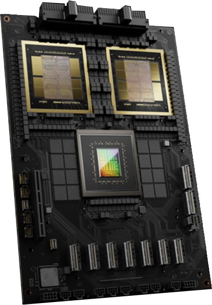
The CPU and GPU Superchip NVIDIA’s approach to scaling AI starts at the level of a single, combined CPU + GPU superchip module. Beginning with the Hopper generation, NVIDIA started packag‐ ing an ARM-based CPU together with one or more GPUs in the same unit, tightly linking them with a high-speed interface. The result is a single module that behaves like a unified computing engine. The first implementation of the superchip was Grace Hopper (GH200), which pairs one Grace CPU with one Hopper GPU. Next came the Grace Blackwell (GB200) Superchip, which pairs one Grace CPU with two Blackwell GPUs in the same pack‐ age. The Grace CPU sits in the center of the module, surrounded by two Blackwell GPU dies, as shown in Figure 2-1.
Figure 2-1. NVIDIA Grace Blackwell Superchip module containing one Grace CPU (cen‐ ter) and two Blackwell B200 GPUs (top left and right) on a single module with a shared unified memory space and connected by a custom high-speed link called NVLink-C2C (chip-to-chip)
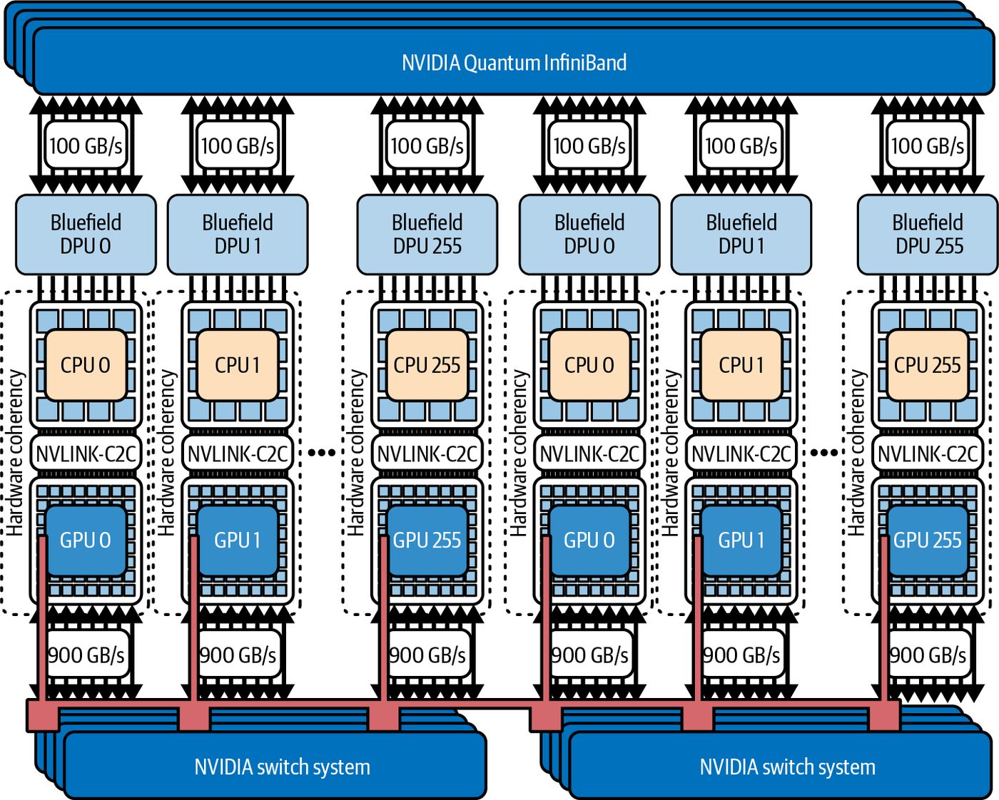
In a traditional system, the CPU and GPU have separate memory pools and commu‐ nicate over a relatively slow bus (like PCIe), which means data has to be copied back and forth. NVIDIA’s superchip eliminates that barrier by connecting the CPU and GPUs with a custom high-speed link called NVLink-C2C (chip-to-chip). NVLink-C2C provides up to ~900 GB/s between the Grace CPU and the Blackwell GPUs in GB200 Superchips. By comparison, PCIe Gen5 x16 (Blackwell B200) is about 64 GB/s per direction, and PCIe Gen6 x16 (Blackwell Ultra B300) is about 128 GB/s per direction. NVLink-C2C’s interconnect speed is an order of magnitude faster than typical PCIe. And, importantly, it is cache-coherent. Cache coherency means the CPU and GPU share a coherent, unified memory archi‐ tecture. As such, they always see the same values. In practice, the Grace CPU and Blackwell GPUs on a superchip can all access one another’s memory directly as if it were one huge memory pool. The GPU can read or write data stored in the CPU’s memory, and vice versa, without needing explicit copies. This unified memory archi‐ tecture is often called Unified CPU-GPU Memory or Extended GPU Memory (EGM) by NVIDIA, and it effectively blurs the line between CPU memory and GPU memory.
24 | Chapter 2: AI System Hardware Overview
Each Grace Blackwell Superchip carries a tremendous amount of memory. The Grace CPU comes with hundreds of gigabytes of LPDDR5X DRAM attached, and each Blackwell GPU has its own high-speed, high-bandwidth memory (HBM) stacks. In the GB200 Superchip, the Grace CPU provides up to ~480 GB of LPDDR5X at up to ~500 TB/s, and the two Blackwell GPUs together contribute up to ~384 GB of HBM3e memory (192 total GB per GPU). In total, a GB200 Superchip exposes roughly ~900 GB of memory of coherent, unified memory accessible by the GPUs and CPUs in a unified address space. To put it simply, each superchip has nearly a terabyte of fast, unified memory at its disposal. This is a game changer for giant AI models. In older systems, a single GPU might be limited to < 100 GB of memory, which meant models larger than that had to be partitioned or offloaded to slower storage. Here, a GPU can seamlessly utilize the CPU’s memory as an extension. If a neural network layer or a large embedding table doesn’t fit in the GPU’s local HBM, it can reside in the CPU’s memory, and the GPU will still be able to work with it across NVLink-C2C. From a programmer’s perspective, the unified virtual address space and coherence simplify correctness. However, for performance, one should explicitly manage placement and memory movement using techniques such as asyn‐ chronous prefetch and staged pipelines. Accessing LPDDR5X using NVLink-C2C has higher latency and roughly an order-of-magnitude lower bandwidth than accessing HBM directly. GPU memory is still much faster and closer to the GPU cores than CPU memory— you can think of the CPU memory as a large but somewhat slower extension. Access‐ ing data in LPDDR5X isn’t as quick as HBM on the GPU. It’s on the order of 10× lower bandwidth and higher latency. A smart runtime will keep the most frequently used data in HBM and use the CPU’s LPDDR5X for overflow or less speed-critical data. The key point is that overflow no longer requires going out to NVMe SSD or across a network. The GPU can fetch from CPU RAM at perhaps 900 GB/s (450 GB/s per direction), which, while slower than HBM, is much faster than fetching from NVMe SSD stor‐ age. This flexibility is critical, as it means a model that is, say, 500 GB in size (too large for a single GPU’s HBM) can still be placed entirely within one superchip module with access to a combined 192 (180 usable) GB in HBM and ~500 GB of CPU mem‐ ory. This model can run without partitioning the model across multiple GPUs. The GPU would just transparently pull the extra data from CPU memory when needed.
The CPU and GPU Superchip | 25
In essence, memory size ceases to be a hard limit for fitting ultralarge models, as long as the total model fits within the combined CPU + GPU memory of the superchip. Many researchers have faced the dreaded “out of memory” errors when models don’t fit on a GPU—this architecture is designed to push that boundary out significantly.
NVIDIA Grace CPU The Grace CPU itself is no sloth. It’s an ARM Neoverse V2 CPU custom-designed by NVIDIA for bandwidth and efficiency. Its job in the superchip is to handle generalpurpose tasks, preprocess and feed data to the GPUs, and manage the mountain of memory attached to it. It runs at a modest clock speed but makes up for it with huge memory bandwidth—up to ~500 GB/s to its LPDDR5X memory—and lots of cache, including over 100 MB of L3 cache. The philosophy is that the CPU should never become a bottleneck when shoveling data to the GPUs. It can stream data from storage or perform on-the-fly data trans‐ formations like tokenization or data augmentation—feeding the GPUs through NVLink-C2C very efficiently. If part of your workload is better on the CPU, the Grace cores can tackle that and make the results immediately accessible by the GPUs. This is a harmonious coupling in which the CPU extends the GPU’s capabilities in areas where GPUs are weaker, like random memory accesses or control-heavy code. And the GPUs accelerate the number-crunching where CPUs can’t keep up. The low-latency link between the CPU and GPUs means they can trade tasks without the usual overhead. For example, launching a GPU kernel from the CPU can happen much faster than on a traditional system, since the command doesn’t have to traverse a slow PCIe bus. The CPU and GPU are essentially on the same board. This is similar to calling a fast local function versus a slower remote function. Next, let’s talk about the Blackwell GPU, the brute-force engine of the superchip.
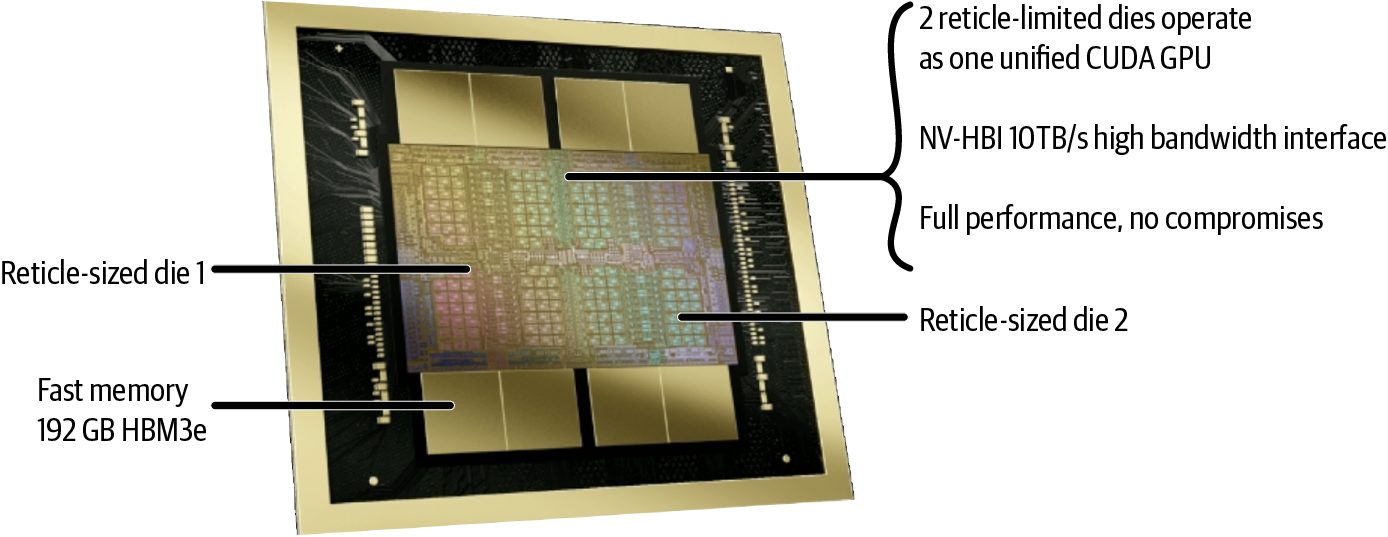
NVIDIA Blackwell “Dual-Die” GPU Blackwell is NVIDIA’s codename for this GPU generation, and it represents a signifi‐ cant leap over the previous Hopper (H100) GPUs in both compute horsepower and memory. The Blackwell B200 and B300 “Ultra” GPU are not single chips. Instead, they use a multichip module (MCM) design with two GPU dies placed in a single module. As such, Blackwell is called a dual-die GPU (see Figure 2-2).
                    While this section dives into the details of the dual-die architecture,
                    the rest of the book will refer to Blackwell’s two combined GPU
                    dies collectively as just the “Blackwell GPU.”
26 | Chapter 2: AI System Hardware Overview
This chiplet approach splits what would normally be one enormous GPU into smaller GPU dies—linking them together with a superfast, on-package die-to-die intercon‐ nect. Why do this? Because a single monolithic die is limited by manufacturing because there’s a limit to how large you can make a chip on silicon. By combining two physical GPU dies into a single module, NVIDIA can double the total transistor budget for the module.
Figure 2-2. Blackwell dual-die multichip module (MCM) design
For the Blackwell B200 MCM, each GPU die has about 104 billion transistors and 96 GB HBM3e memory. The combined GPU module has around 208 billion transistors and 192 (180 usable) GB total memory per B200 GPU. By comparison, the Hopper H100 GPU had ~80 billion transistors and 80 GB HBM3 (versus Blackwell’s HBM3e) memory. As such, Blackwell’s B200 more than doubles transistor count and ~2.4× increases memory size. Blackwell’s two GPU dies communicate using a specialized, high-speed 10 TB/s dieto-die interconnect called NV-HBI (High-Bandwidth Interface). This lets the two GPU dies in the module function as a single unified GPU. The software layer running on top of it sees only a single GPU. From the system’s perspective, a Blackwell GPU is one single module, or device, with a large pool of memory (192 [180 usable] GB HBM3e) and a ton of execution units, but under the hood it’s two chips working in tandem. NVIDIA’s software and sched‐ uling ensure that work is balanced across the two GPU dies and memory accesses are coherent. This allows developers to largely ignore this complexity, as they appear as one GPU, as NVIDIA intended. Each Blackwell B200 GPU module has 192 (180 usable) GB of HBM3e memory com‐ bined across the two GPU dies (96 GB each) and divided into 8-Hi stacks. An 8-Hi HBM3e stack is built by vertically stacking eight DRAM dies—each 3 GB—for a total of 24 GB per stack.
The CPU and GPU Superchip | 27
The B200 GPU uses eight of these stacks (four per die) to provide 192 (180 usable) GB (192 GB = 8 stacks × 24 GB per stack) of on-package memory. This increases the per-GPU stack count and capacity compared to the previous generation Hopper GPUs—and gives more headroom for model parameters, activations, gradients, and input data.
                   Only 180 GB of the 192 GB HBM3e memory is usable per B200
                   due to error correcting code (ECC), system firmware usage, manu‐
                   facturing limitations, and other issues that prevent the chip from
                   exposing the full 192 GB. As such, we’ll reference 180 GB instead of
                   the full 192 GB for the Blackwell B200 available memory.
The memory is also faster, as Blackwell’s B200 HBM3e has an aggregate bandwidth up to roughly 8 TB/s per GPU. For comparison, the Hopper uses the previous genera‐ tion HBM3, which delivers ~3.35 TB/s per GPU. As such, Blackwell’s memory band‐ width throughput is roughly 2.4× higher than Hopper’s. Feeding data at 8 terabytes per second, the Blackwell GPU cores are kept busy crunching on huge matrices without frequently stalling to wait for data. NVIDIA also beefed up on-chip caching, as Blackwell has a total of 126 MB of L2 cache (63 MB per die). This cache is a small but ultrafast memory on the GPU that holds recently used data. By increasing the L2 cache size by more than 2.5× compared to Hopper’s 50 MB L2 cache, Blackwell can keep more of the neural network weights or intermediate results on chip, avoiding extra trips out to HBM. This again helps ensure the GPU’s compute units are seldom starved for data. Next, let’s show how the Blackwell GPU is paired with a dedicated set of reducedprecision Tensor Cores—as well as transformer-optimized hardware and software APIs from NVIDIA called the Transformer Engine. Frameworks, like PyTorch and inference engines like vLLM, support these optimizations by using libraries like CUDA, CUTLASS, and OpenAI’s Triton, which we talk about in later chapters.
                   Remember that the rest of this book refers to Blackwell’s dual-die
                   GPU as just the “Blackwell GPU.”
28 | Chapter 2: AI System Hardware Overview
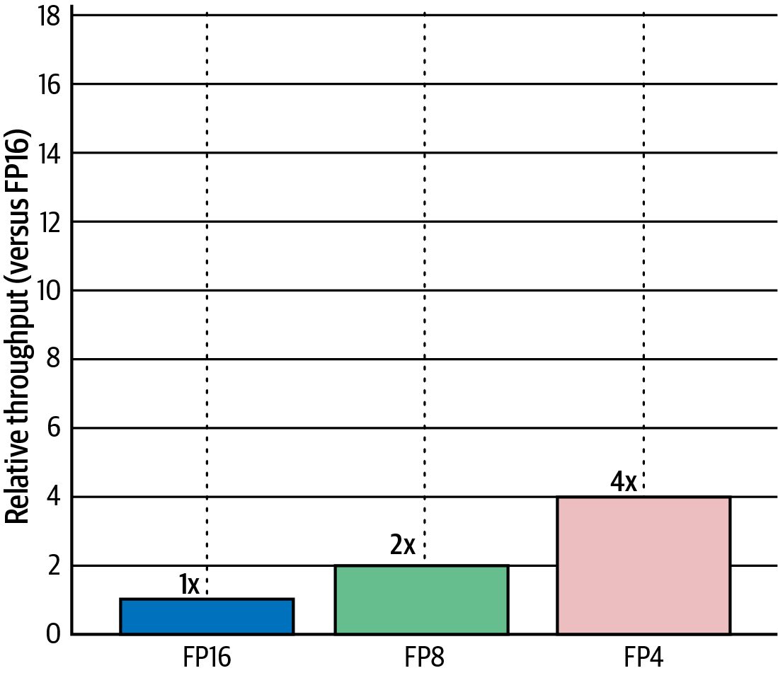
NVIDIA GPU Tensor Cores and Transformer Engine Speaking of compute units, Blackwell introduces enhancements specifically aimed at AI workloads. Central to this is NVIDIA’s Tensor Core technology and the Trans‐ former Engine (TE). Tensor Cores are specialized units within each streaming multi‐ processor (SM) of the GPU that can perform matrix multiplication operations at very high speed. Tensor Cores were present in prior generations, but Blackwell’s Tensor Cores support even more numerical formats, including extremely low-precision ones like 8-bit and 4-bit floating point. The idea behind lower precision is simple. By using fewer bits to represent numbers, you can perform more operations at the same time—not to men‐ tion your memory goes further since fewer bits are used to represent the same num‐ bers. This assumes that your algorithm can tolerate a little loss in numerical precision. These days, a lot of AI algorithms are designed with low-precision numeri‐ cal formats in mind. NVIDIA pioneered the TE to automatically adjust and use mixed precision in deep learning where critical layers use higher precision (FP16 or BF16) and less critical lay‐ ers use FP8. TE automatically optimizes the balance of precision with the goal of maintaining the model’s accuracy at the lower precision. In the Hopper generation, the TE first introduced FP8 support, which doubled the throughput versus FP16. Blackwell takes it one step further by introducing NVIDIA FP4 (NVFP4), a 4-bit floating-point format that uses half the number of bits of FP8. FP4 is so small that it can potentially double the compute throughput of FP8. Figure 2-3 shows the relative speedup of FP8 and FP4 compared to FP16. An entire NVL72 rack (72 GPUs) has a theoretical Tensor Core throughput over 1.4 exaFLOPS (that’s 1.4 × 10¹⁸) in 4-bit precision. This is a mind-boggling number that puts this single rack in the realm of the world’s fastest supercomputers—albeit at low FP4 precision. Even if real-world workloads don’t always hit that peak, the capability is there, which is astonishing. Modern GPUs use a TE that adds NVFP4 support together with improved scaling and calibration. In practice, you adopt TE by using its kernels and modules in frame‐ works such as PyTorch. This way, FP8 and NVFP4 are applied when they preserve accuracy. This is not a fully automatic per-layer decision in all frameworks.
The CPU and GPU Superchip | 29
Figure 2-3. Relative speedup of FP8 and FP4 compared to FP16
Advanced techniques include dynamically changing the precision for each layer of a neural network during training and inference. The goal is to use the lowest precision that will still preserve model accuracy for each of those layers. For example, the TE might keep the first layers of a neural net in FP16 since early layers can be sensitive to noise. But, based on heuristics, it could decide to use FP8 or FP4 for later layers that are more tolerant—or for giant embedding matrices where high precision isn’t as critical. All of this can happen under the hood in NVIDIA libraries and AI frameworks like PyTorch. As a user, you just enable mixed precision, and the result is a huge speedup that essentially comes “for free.” We’ll discuss mixed precision in Chapter 9, but just know that many LLMs today use mixed precision for this reason. These reduced pre‐ cisions improve training speed compared to FP16 and FP32—and reduce accuracy loss. Blackwell was built to make FP8 and FP4 accessible and efficient. These reduced-precision formats reduce memory usage as well. Using FP4 halves the memory needed per parameter compared to FP8 (and FP8 halves FP16 memory usage), meaning you can pack an even larger model into the GPU’s memory. NVIDIA has effectively bet on AI’s future being in lower precision arithmetic and has given Blackwell the ability to excel at it. This is especially critical for inference serving of massive models, where throughput (tokens per second) and latency are paramount.
30 | Chapter 2: AI System Hardware Overview
To illustrate the generational leap forward from Hopper to Blackwell, NVIDIA reported an H100-based system could generate only about 3.4 tokens per second per GPU for a large 1.8-trillion-parameter MoE model—with over 5 seconds of latency for the first token. This is too slow for interactive use. The Blackwell-based system (NVL72) ran the same model with around 150 tokens per second per GPU and a low first-token latency of ~50 milliseconds. That is roughly 30× the real-time throughput improvement over the Hopper generation. The NVL72 allowed this massive model to serve real-time responses—opening it up to many more low-latency use cases. This speedup came from raw FLOPS, the combination of faster GPUs, lower preci‐ sion (FP4) usage, and the NVLink interconnect keeping the GPUs fed with data. It underscores how a holistic design that spans across both compute and communica‐ tion can translate into real-world performance gains. In essence, Blackwell GPUs are more powerful, smarter, and better fed with data than their predecessors. They chew through math faster, thanks to Tensor Cores, TE, and low precision. Additionally, the system architecture ensures that data is made avail‐ able quickly thanks to huge memory bandwidth, large caches, and NVLink. Before moving on, let’s quickly discuss the hierarchy inside the GPU, as this is useful to understand performance tuning later.
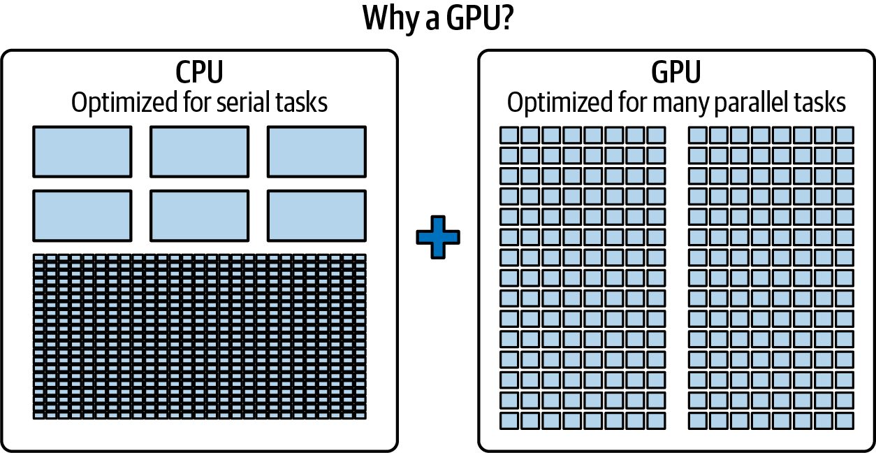
Streaming Multiprocessor, Threads, and Warps Each Blackwell GPU, like its predecessors, consists of many streaming multiproces‐ sors (SMs). Think of these like the “cores” of the GPU, as shown in Figure 2-4.
Figure 2-4. Comparing CPU cores to GPU cores (source: https://oreil.ly/003EH, https:// oreil.ly/Z25Tf)
The CPU and GPU Superchip | 31
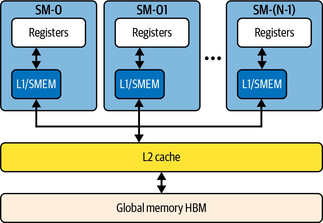
Each SM contains a bunch of arithmetic units (for FP32, INT32, etc.), Tensor Cores for matrix math, load/store units for memory operations, and some special function units for things like transcendental math. The GPU also has its own small pool of superfast memory, including registers, shared memory, and L1 cache. An SM executes threads in fixed-size groups known as warps, with each warp con‐ taining exactly 32 threads that execute the exact same instructions in lockstep. This is called the single instruction, multiple threads (SIMT) execution model. SMs execute many active warps in parallel to help cover the latency of a thread wait‐ ing on data accessed from global memory. Consider an SM having dozens of warps (hundreds of threads) in flight concurrently. If one warp is waiting on a memory fetch, another warp can run. This is called latency hiding. We will revisit latency hid‐ ing throughout the book. This is a very important performance-optimization tool to have in your tuning toolbox. A high-end GPU like Blackwell will have hundreds of SMs. Each SM is capable of running thousands of threads concurrently. This is how we get tens of thousands of active threads onto a single GPU. All those SMs share a 126 MB L2 cache, as we men‐ tioned earlier, and share the memory controllers that connect to the HBM. The mem‐ ory hierarchy contains registers (per thread) → shared memory (per thread block, on each SM) → L1 cache (per SM) → L2 cache (shared across all SMs on the GPU) → HBM memory (off chip), as shown in Figure 2-5.
Figure 2-5. GPU memory hierarchy
32 | Chapter 2: AI System Hardware Overview
For best performance, data needs to stay as high in that hierarchy as possible. If every operation went out to HBM even at 8 TB/s, the GPU would stall too often due to the increased latency of accessing off-chip memory. By keeping reusable data in SM local memory or L2 cache, the GPU can achieve enormous throughput. The Blackwell architecture’s doubling of cache and bandwidth is aimed exactly at keeping the GPU beast fed and happy. As performance engineers, we’ll see many examples where a kernel’s performance is bound by compute as well as memory traffic and throughput. NVIDIA clearly designed Blackwell so that, for many AI workloads, the balance between FLOPS and memory bandwidth is well-matched. Blackwell’s design balances compute and memory so that for many AI kernels the GPUs can keep computing with minimal stalls. In practice, well-optimized dense math operations can reuse data from on-chip memory to approach peak FLOPS without being severely memory bound. All of this means that, given well-optimized code, the GPUs will often be busy com‐ puting rather than waiting on data. Note that certain operations like huge reductions or random memory accesses can still be memory bound, but the updated GPU, mem‐ ory, and interconnect hardware make this a bit less of an issue.
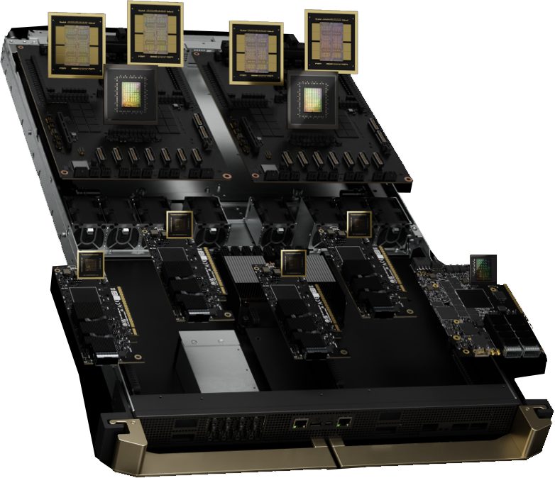
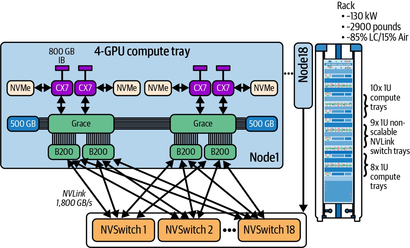
Ultrascale Networking Treating Many GPUs as One Packing two GPUs and a CPU into a superchip gives us an incredibly powerful node. The next challenge is connecting many of these superchips together to scale out to even larger model training. NVIDIA provides a large rack configuration using GB200/GB300 Superchips called the NVL72 system. NVL72 stands for a system with 72 Blackwell GPUs—and 36 Grace CPUs—all interconnected with NVLink. This is essentially an AI supercom‐ puter in a single rack. The GB200/GB300 NVL72 is built as 18 compute nodes in which each node contains two GB200/GB300 Superchips for a total of four Blackwell GPUs + two Grace CPUs per compute node, as shown in Figure 2-6.
Ultrascale Networking Treating Many GPUs as One | 33
Figure 2-6. A 1U compute tray within the GB200/GB300 NVL72 rack with two Grace Blackwell Superchips (source: developer.nvidia.com)
Here, each superchip module has one Grace CPU and two Blackwell GPUs (each B200 is a dual-die MCM). The NVL72 has 18 of these trays linked together. By con‐ necting the 18 compute nodes together, the GB200/GB300 NVL72 links 72 Blackwell GPUs (18 nodes × 4 GPUs) and 36 Grace CPUs (18 nodes × 2 CPUs) together to form a powerful, unified CPU-GPU cluster. The interesting thing about the NVL72 is that every GPU can talk to any other GPU through the NVLink Switch fabric at very high speed within a single NVLink domain. NVIDIA achieved this using a combination of NVLink 5 connections on the GPUs and a dedicated switch silicon called NVSwitch.
NVLink and NVSwitch Each Blackwell GPU exposes 18 NVLink 5 ports. Aggregate bidirectional NVLink bandwidth is 1.8 TB/s per GPU (18 NVLink links × 100 GB/s bidirectional) with the NVL72 wiring all ports to the NVLink Switch System. Each NVLink switch tray delivers 144 NVLink ports at 100 GB/s. Across the nine trays, each GPU’s 18 NVLink 5 links are wired one per NVSwitch chip so the 72 GPUs are fully connected at full bisection bandwidth. The aggregate bidirectional NVLink 5 bandwidth is 1.8 TB/s per GPU (18 NVLink links × 100 GB/s bidirectional).
34 | Chapter 2: AI System Hardware Overview
This is double the per-GPU NVLink bandwidth of the previous generation used by Hopper GPUs. The Hopper H100 uses 18 NVLink 4 ports but runs at half the speed of NVLink 5. Inter-GPU latency over NVLink is in the single-digit microsecond range. The GPUs are cabled in a network through NVSwitch chips. NVSwitch is essentially a switching chip similar to a network switch, but it’s built specifically for NVLink. This means any GPU can reach any other GPU through one switch stage in the NVLink Switch System at full bisection bandwidth. This one-stage property holds true within a single NVL72 rack because each GPU uses its 18 NVLink links to connect to the 18 NVSwitch chips, enabling a path through a single switch. Figure 2-7 shows an NVLink Switch tray used in NVL72.
Figure 2-7. One NVLink Switch tray inside the NVL72 (source: https://oreil.ly/h7seG)
Each switch tray contains two NVSwitch chips and multiple high-speed ports. The NVL72 rack comprises 9 such switch trays and 18 compute trays, as shown in Figure 2-8.
Ultrascale Networking Treating Many GPUs as One | 35
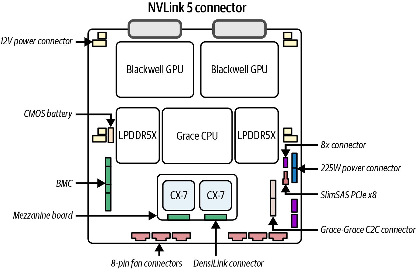
Figure 2-8. NVSwitch System of nine trays inside an NVL72 rack (source: https:// oreil.ly/h7seG)
36 | Chapter 2: AI System Hardware Overview
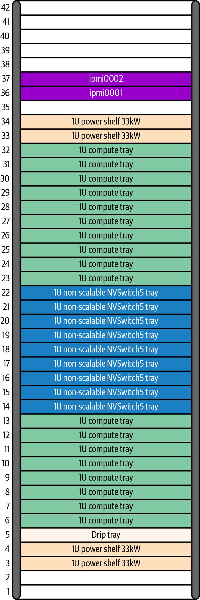
Since each of the 9 switch trays contains two NVSwitch chips, the total is 18 NVSwitch chips in the NVL72 system. The network is arranged as a full crossbar such that every GPU is connected to every NVSwitch, and every NVSwitch is con‐ nected to every GPU. This provides a high-bandwidth path between any pair of GPUs. Each switch tray exposes 144 NVLink ports to fully connect the 18 NVLink links on each GPU. Concretely, each GPU uses its 18 NVLink links to connect to the 18 NVSwitch chips (one link to each switch). This means any GPU can reach any other GPU in one hop (GPU → NVSwitch → GPU), with enormous bandwidth along the way. Figure 2-9 shows the full NVL72 architecture with 72 fully connected GPUs (36 GB200 superchips) and 18 NVSwitches.
Figure 2-9. Each GPU connects to each NVSwitch (one link for each switch)
The aggregate bisection bandwidth across the entire 72-GPU network is about 130 TB/s within an NVL72 rack. For perspective, that is many times higher than even a top-end InfiniBand cluster of similar scale. The design exposes a fully connected, high-bandwidth fabric with a global address space across GPUs. This allows efficient collectives and one-sided operations while preserving explicit software control over synchronization and consistency.
Ultrascale Networking Treating Many GPUs as One | 37
Multi-GPU Programming From a programming model standpoint, one GPU can directly access another GPU’s memory over NVLink using peer-to-peer and partitioned global address space (PGAS) models such as NVIDIA SHMEM (NVSHMEM), NVIDIA’s GPU-accelerated OpenSHMEM implementation. There is a global address space, but GPU caches are not globally coherent across GPUs. Only the CPU–GPU path over NVLink-C2C is cache coherent. Software stacks such as NCCL and NVSHMEM provide the synchro‐ nization and ordering required for correct multi-GPU access. Combined, hardware cache coherency and software synchronization techniques allow the NVL72 to be seen as essentially one big GPU. Remote direct memory access (RDMA) is a network technology that enables direct, zero-copy memory transfers between hosts across InfiniBand and RDMA over Con‐ verged Ethernet (RoCE) transports. Optional remote atomic operations are defined by the InfiniBand Trade Association (IBTA) for InfiniBand and RoCE. GPUDirect RDMA, NVIDIA’s implementation of the RDMA protocol, enables net‐ work interface controllers (NICs) to register GPU memory and perform RDMA directly to and from GPU memory using the nvidia-peermem driver. This allows GPUs to exchange data and execute atomic operations across nodes without involv‐ ing the CPU. This allows NICs to perform direct DMA to and from GPU memory without staging through host RAM. Remote atomics and one-sided operations across nodes are provided by upper-layer libraries such as NVSHMEM, which implement these semantics over RDMA trans‐ ports. Note that GPUDirect RDMA supplies the direct data path rather than the atomic APIs themselves. Distributed training and inference workloads need to syn‐ chronize and exchange information frequently across many GPUs. Traditionally, the GPUs are in different compute nodes and racks. As such, synchro‐ nization can happen over relatively slow network links like InfiniBand and Ethernet. This is often the bottleneck when scaling across many GPUs to support large AI models. With an NVL72 system, those exchanges happen over NVLink and NVSwitch at a superfast pace. This means you can scale your training job or inference cluster up to 72 GPUs with minimal communication overhead. And since the GPUs spend far less time waiting for data from one another, overall throughput scales near-linearly up to 72 GPUs.
38 | Chapter 2: AI System Hardware Overview
In contrast, consider scaling the same job across a similarly sized 72-GPU H100 clus‐ ter of nine separate compute servers—each with eight Hopper H100 GPUs. This con‐ figuration requires InfiniBand, which will create network bottlenecks that greatly reduce the cluster’s scaling efficiency. Let’s analyze and compare the NVL72 and 72-GPU H100 clusters using concrete numbers. Within a single NVL72 rack, GPU-to-GPU bandwidth is up to 1.8 TB/s per GPU (bidirectional aggregate), and latency is on the order of 1–2 microseconds for a small message on the order of kilobytes. Large messages take longer and are typically bandwidth-limited. Across a conventional InfiniBand network, bandwidth per GPU might be more like 20–80 GB/s—depending on how many NICs and their speed— and latency is likely 5–10 microseconds or more. The NVL72 network offers substantially higher per-GPU bandwidth and lower latency than host-NIC fabrics. Specifically, NVLink 5 provides about 1.8 TB/s of aggregate bandwidth per GPU, whereas modern host NICs provide about 50–100 GB/s per port at 400–800 Gb/s line rates. All of this decreases collective-operation overhead down from tens of percent down to just a few percent. In practical terms, collective overhead is substantially lower within an NVLinkconnected NVL72 system versus a traditional node-to-node fabric, but the exact frac‐ tion of iteration time is workload-dependent. For example, NVIDIA reported that a 1.8-trillion-parameter MoE model improved from about 3.4 tokens per second per GPU with over 5 seconds time to first token on H100 to about 150 tokens per second per GPU with roughly 50 ms time to first token on GB200 NVL72. This speedup is largely due to eliminating inter-GPU communication bottlenecks inside the NVL72 rack in addition to Blackwell’s higher compute throughput. Within a single NVL72 rack, communication is so fast that communication bottle‐ necks become low priority as they are almost completely eliminated, whereas com‐ munication in traditional InfiniBand and Ethernet clusters is often the primary bottleneck and needs careful optimization and tuning at the software level. In short, you should design and implement software that exploits the NVL72 config‐ uration by keeping as much of the workload’s communication inside the rack (“intrarack”) as possible to take advantage of the high-speed NVLink and NVSwitch hardware. Use the slower InfiniBandor Ethernet-based communication between racks (“inter-rack”) only when absolutely necessary to scale beyond the NVL72’s compute and memory resources.
Ultrascale Networking Treating Many GPUs as One | 39
In-Network Aggregations with NVIDIA SHARP Another hardware-enabled optimization is NVIDIA Scalable Hierarchical Aggrega‐ tion and Reduction Protocol (SHARP). For NVLink Switch System racks, in-network reductions use SHARP engines integrated into NVSwitch ASICs to offload reductions and other collectives in-network (see Figure 2-10).
Figure 2-10. Offloading computations to the NVIDIA network hardware using SHARP reduction engines in NVSwitch
The NVSwitch fabric combines partial results without the data needing to funnel through the GPUs. By offloading collective computations from the GPUs to the switch hardware itself, SHARP allows the GPUs to focus on more complex computa‐ tions, lowers collective latencies, reduces the overall volume of data traversing the network, and increases system efficiency. SHARP’s increased efficiency means that during distributed training, the heavy lifting of aggregating gradients or synchronizing parameters is handled by the NVSwitch’s dedicated SHARP engines. The result is much more efficient scaling across both intra-rack and inter-rack configurations.
40 | Chapter 2: AI System Hardware Overview
With SHARP, you’ll see near-linear performance improvements even as the number of GPUs grows. This in-network computing capability is especially critical for train‐ ing ultralarge models, where every microsecond saved on collective operations can translate into substantial overall speedups.
               SHARP is one of the most impactful innovations that NVIDIA
               received during their 2019–2020 acquisition of Mellanox. You
               should explore SHARP if you are not currently using it. SHARP
               can significantly reduce latency and traffic for collectives and often
               improves scaling efficiency for communication-bound training.
Multirack and Storage Communication Next, let’s discuss how an NVL72 rack talks to another NVL72—or to an external storage system like a shared filesystem. As we have shown, inside the NVL72 rack, NVLink covers all GPU-to-GPU traffic. But outside the rack, it relies on more tradi‐ tional networking hardware. Each compute node in NVL72 is equipped with high-speed Network Interface Cards and a Data Processing Unit (DPU). A DPU offloads, accelerates, and isolates net‐ working, storage, security, and management tasks from the host CPU. By running these operations directly on the NIC, DPUs reduce CPU overhead and latency. In the NVL72 design, the BlueField-3 DPU handles line-rate packet processing, RDMA, and NVMe over Fabrics (oF) operations. NVMe-oF is a protocol variant of NVMe that extends storage across network fabrics. As such, the DPU moves data directly between the network, storage, and GPU memory without CPU involvement. This maximizes overall system throughput and efficiency. GB200/GB300 NVL72 racks integrate with Quantum-X800 InfiniBand or SpectrumX800 Ethernet fabrics. The compute trays commonly use four ConnectX-8 800 Gb/s NICs per node for high external bandwidth. BlueField-3 DPUs are used where innetwork acceleration or offload is required for storage, security, and control-plane tasks. With four 800 Gb/s NICs, it is 3.2 Tbit/s per compute node and about 57.6 Tbit/s per rack (57.6 Tbit/s = 3.2 Tbit/s per node × 18 nodes). While this throughput is eyepopping, remember that when you exit the rack, you still need an ultrafast network. This way, multirack scaling isn’t bottlenecked at the rack boundary. NVIDIA calls these multirack deployments AI factories. And they’ve made sure that the NVL72 can plug into a larger network fabric using these four NICs per node. The BlueField-3 DPU in each node helps offload networking tasks like RDMA, TCP/IP, and NVMe SSD storage access. This makes sure the Grace CPU isn’t bogged down managing network interrupts. The DPU essentially serves as a smart network
Ultrascale Networking Treating Many GPUs as One | 41
controller, moving data directly between NICs and GPU memory using NVIDIA’s GPUDirect RDMA software. This does not require staging data through host mem‐ ory or using any CPU cycles. BlueField DPUs avoid CPU involvement, which is especially useful when streaming large datasets from a storage server for large-scale training jobs. Specifically, the DPU can handle the transfer and deposit data directly into GPU memory—while the CPU focuses on other tasks like data preprocessing. In addition to providing performance-offload capabilities, the DPU supports secure multitenancy. It isolates network traffic for different jobs and users—acting as a smart firewall/switch on the node. When scaling out to multiple NVL72 racks, NVIDIA uses Quantum-series InfiniBand switches. Multiple NVL72 racks can be interconnected using these InfiniBand switches to form a large cluster of NVL72 racks. For example, an 8-rack NVL72 totaling 576 GPUs is connected as one NVLink 5 domain using the NVLink Switch System. InfiniBand or Ethernet is then used to con‐ nect that NVLink domain to other domains (e.g., other NVL72 racks) or to external storage (though the performance for cross-rack InfiniBand or Ethernet communica‐ tion will be lower than the intra-rack NVLink/NVSwitch communication). In short, InfiniBand and Ethernet NICs such as NVIDIA’s ConnectX and BlueField DPU are typically used alongside NVLink. These provide high-bandwidth connectiv‐ ity between racks and also offload protocols using in-network computing on DPUs.
Preintegrated Rack Appliance Because NVL72 is such a complex system, NVIDIA delivers it as a preintegrated rack “appliance” in a single cabinet. It comes assembled with all 18 compute nodes, all 9 NVSwitch units, internal NVLink cabling, power distribution, and a cooling system. The idea is that an organization can order this as a unit that is ready to go when it arrives. One simply connects the rack to facility power, hooks up the water cooling interfaces, connects the InfiniBand cables to your network, and powers it on. The system is essentially ready for use out of the box, requiring only minimal setup to begin running AI workloads. There is no need to individually cable 72 GPUs with NVLink, as NVIDIA has already done this inside the rack for you. Even the liquid cooling setup is self-contained, as we’ll discuss soon. This appliance approach accelerates deployment and ensures that the system is built correctly and validated by NVIDIA. The rack also includes its NVIDIA Base Com‐ mand Manager cluster-management software—as well as the Simple Linux Utility for Resource Management (SLURM) and Kubernetes for cluster-job scheduling and orchestration.
42 | Chapter 2: AI System Hardware Overview
In short, the NVL72 rack is designed to be dropped into your environment and ready to run production AI workloads right out of the box. It doesn’t need any manual installation or complex configuration.
Co-Packaged Optics: Future of Networking Hardware As networking data throughput rates climb to 800 Gbit/s, 1.6 Tbit/s, and beyond, NVIDIA has begun integrating silicon photonics and co-packaged optics (CPO) into its networking hardware. This includes the Quantum-X800 InfiniBand and Spectrum-X800 Ethernet platforms. These platforms ship with 800 Gb/s end-to-end connectivity and in-network computing features (e.g., SHARP). With CPO, the opti‐ cal transmitters are integrated right next to the switch silicon. This drastically short‐ ens electrical pathways, enabling even higher bandwidth links between racks, reducing power draw, and improving overall communication efficiency. In practical terms, technologies like CPO are paving the way to connect hundreds and thousands of racks (AI factories) into a single unified fabric in which inter-rack bandwidth is no longer the bottleneck. Such optical networking advancements are crucial to the high-performance, inter-rack bandwidth needed to ensure that the net‐ work can keep up with the GPUs at ultrascale. To summarize, inside an NVL72 rack, NVIDIA uses NVLink and NVSwitch to create a blazingly fast, all-to-all connected network between 72 GPUs. These interconnects are so fast and uniform that the GPUs effectively behave like one unit for many col‐ lective operations. Beyond the rack, high-speed NICs (e.g., InfiniBand or Ethernet) connect the rack to other racks or to storage, with DPUs to manage data movement efficiently. The NVL72 is an immensely powerful standalone system and a basic building block for larger AI supercomputers or AI factories. The concept of an AI factory, a largescale AI data center composed of multiple such racks, is now becoming reality. NVI‐ DIA partners with OEM and system vendors like HPE and Supermicro to supply the GB200 NVL72 systems. NVIDIA’s hardware and network roadmaps are squarely aimed at enabling the AI factory vision. In short, the NVL72 shows how far codesign can go as the GPU, networking, and physical-rack hardware are built hand in hand to scale to thousands and millions of GPUs as seamlessly and efficiently as possible.
Compute Density and Power Requirements The NVL72 rack is incredibly dense in terms of compute, which means it draws a very high amount of power for a single rack. A fully loaded NVL72 can consume up to ~130 kW of power under max load. This is more than 2× NVIDIA’s previous gen‐ eration AI rack, which consumed around 50–60 kW. Packing 72 bleeding-edge
Compute Density and Power Requirements | 43
GPUs—and all the supporting hardware—into one rack pushes the limits of what data center infrastructure can handle. To supply 130 kW to the NVL72 rack, you can’t just use a single standard power feed. Data centers will typically provision multiple high-capacity circuits to feed this kind of power. For instance, a data center can deploy two fully independent power feeds. In this case, each feed is sized to carry the entire rack load in case of a failure on one of the feeds. If one feed goes offline, the remaining circuit can support the full 130 kW draw to avoid a blown circuit. This kind of redundancy is important protection. Otherwise, the power interruption could halt your multimonth training job. Within the rack, power is distributed to the power supplies of each 1U compute node. The power is converted from AC to DC for the local electronics. Each compute node in the NVL72 contains two Grace Blackwell Superchips, which together consume on the order of 6 kW. With 18 compute nodes, the total power consumed is ~110 kW. The NVSwitch trays, network switches, air cooling, and water cooling pumps account for ~20 kW for a total of 130 kW consumed by the entire NVL72 rack. The current used at a typical data center in voltages (e.g., 415 V 3-phase AC) is mas‐ sive, so everything is engineered for high amperage. Operators have to carefully plan to host such a rack, which often requires dedicated power distribution units (PDUs) and careful monitoring. Power transients are also a consideration, as 72 GPUs, when ramping from idle to full power, could rapidly draw tens of kW of power in just milli‐ seconds. A good design will include capacitors or sequencing to avoid large voltage drops. The system might stagger the GPU boost clocks by tiny intervals so they don’t all spike at exactly the same microsecond, smoothing out the surge. These are the kind of electrical engineering details that go into making a 130 kW rack manageable. It’s not far-fetched to call this NVL72 rack, at the cutting edge of high-density com‐ pute, a mini power substation. Eight of these racks combined for 576 GPUs would draw nearly 1 MW of power (8 racks × 130 kW per rack), which is the entire capacity of a small data center! The silver lining is that although 130 kW is a lot in one rack, you are also getting a lot of work done per watt. If one NVL72 replaces several racks of older equipment, the overall efficiency is bet‐ ter. But you definitely need the infrastructure to support that concentrated power draw. And any facility hosting the NVL72 racks must ensure they have adequate power capacity and cooling, as we will discuss next.
44 | Chapter 2: AI System Hardware Overview
Liquid Cooling Versus Air Cooling Cooling 130 kW in one rack is beyond the reach of traditional air cooling. Blowing air over 72 GPUs that each can dissipate ~1,200 watts would require hurricane-like airflow and would be extremely loud and inefficient—not to mention the hot air exhaust would be brutal. As such, liquid cooling is the only practical solution for the NVL72 rack running at this power density. The NVL72 is a fully liquid-cooled system. Each Grace Blackwell Superchip module and each NVSwitch chip has a cold plate attached. A cold plate is a metal plate with internal tubing that sits directly on the component. A water-based coolant liquid flows through the tubing to carry away heat. All these cold plates are linked by hoses, manifolds, and pumps that circulate the coolant throughout the system. Typically, the rack will have quick-disconnect couplings for each node so you can slide a server in or out without spilling the coolant. The rack then has supply and return connections to the external facility’s chilled water system. Often, there’s a heat exchanger called a Coolant Distribution Unit (CDU) either built into the rack or immediately next to it. The CDU transfers heat from the rack’s internal coolant loop to the data center’s water loop. The facility provides chilled water at 20–30°C. The water absorbs the heat through the heat exchanger. The warmed-up water is then pumped back into the chillers or cooling towers to be cooled again. In modern designs, they might even run warm water cooling, in which chilled water comes into the system at 30°C and leaves at 45°C. The water can then be cooled by evaporative cooling towers without active refrigeration, improving overall efficiency. The point is, water, or a liquid coolant, can carry far more heat per unit of flow than air, so liquid cooling is vastly more effective when running at high watts in small spaces. By keeping the GPU and CPU temperatures much lower than they would be with air, liquid cooling reduces thermal GPU throttling. The GPUs can sustain their maxi‐ mum clocks without hitting temperature limits. Also, running chips cooler improves reliability and even efficiency since power leakage is lower when running at lower temperatures. The NVL72 keeps GPU temps in the 50–70°C range under load, which is excellent for such power-hungry devices. The cold plates and coolant loops have been engineered very carefully to allow each GPU to dump 1,000 W and each CPU to dump 500 W into the system. In addition, the coolant flow rate has to be sufficient to remove that heat quickly. A rough estimate shows on the order of 150–200 liters per minute at a 10–12°C water temperature rise to dissipate about 130 kW.
Liquid Cooling Versus Air Cooling | 45
The system undoubtedly has sensors and controls for coolant temperature, pressure, and leak detection. If a leak is detected from its drip or pressure-loss sensors, the sys‐ tem can shut down or isolate that section quickly. It’s recommended to use selfsealing connections—and perhaps a secondary containment tray—to minimize the risk of leaking fluids. This level of liquid cooling in racks was once exotic, but it is now the standard for these large-scale AI clusters. Companies like Meta, xAI, and Google are adopting liq‐ uid cooling for their AI clusters because air cooling simply cannot support the large amount of power drawn from these systems. So while an NVL72 requires more facility complexity, including liquid-cooling loops, many data centers are now built with liquid cooling in mind. The NVL72 rack, with its built-in internal liquid cooling, can be connected directly to the cooling loop. One side effect of the internal liquid cooling is the weight of the rack. The NVL72 rack weighs on the order of 3,000 lbs (1.3–1.4 metric tons) when filled with hardware and coolant. This is extremely heavy for a rack, as it’s roughly the weight of a small car but concentrated on a few square feet of floor. Data centers with raised floors have to check that the floor can support this load, measured in pounds per square foot. Often, high-density racks are placed on reinforced slabs or supported by additional struts. Moving such a rack requires special equipment such as forklifts. This is all part of the deployment consideration, as you’re installing an AI supercomputer, which comes with its unique physical and logistical challenges. NVIDIA also integrates management and safety features in the form of a rack man‐ agement controller that oversees things like coolant pumps, valve positions, and power usage, and monitors every node’s status. Administrators can interface with it to do things like update firmware across all nodes, or to shut down the system safely. All these considerations illustrate that the NVL72 was codesigned with data center infrastructure in mind. NVIDIA worked on the compute architecture in tandem with system engineers who figured out power delivery and cooling, and in tandem with facility engineers who specified how to install and run these things. It’s not just about fast chips—it’s about delivering a balanced, usable system. The payoff for this complexity is huge. By pushing the limits of power and cooling, an enormous, amount of compute is concentrated into a single rack and translates to a large amount of compute-per-watt. Yes, 130 kW is a lot of power, but per GPU or per trillion FLOP (TFLOP), it’s actually efficient compared to spreading the same GPUs across multiple racks with less efficient cooling.
46 | Chapter 2: AI System Hardware Overview
Performance Monitoring and Utilization in Practice When you have a machine this powerful, you want to make sure you’re getting the most out of it. Operating an NVL72 effectively requires careful monitoring of perfor‐ mance, utilization, and power. NVIDIA provides tools like Data Center GPU Man‐ ager (DCGM) that can track metrics on each GPU for things like GPU utilization percentage, memory usage, temperature, and NVLink throughput. As a performance engineer, you’d keep an eye on these during training runs and inference workloads. Ideally, you want your GPUs to be near 100% utilized most of the time during a training job. If you see GPUs at 50% utilization, that means some‐ thing is keeping them idle for half the time. Perhaps there is a data loading bottleneck or a synchronization issue. Similarly, you can monitor the NVLink usage. If your NVLink links are saturating frequently, communication is likely the culprit. The BlueField DPUs and NICs have their own statistics that are monitored to ensure that you’re not saturating your stor‐ age links when reading data. Modern systems like the NVL72 expose this telemetry. Power monitoring is also crucial. At ~130 kW, even a small inefficiency or misconfi‐ guration can waste a lot of power and money. The system likely lets you monitor power draw per node or per GPU. Administrators might cap the power or clocks of GPUs if full performance isn’t needed, to save energy. NVIDIA GPUs allow setting power limits. For instance, if you’re running a smaller job that doesn’t need every last drop of performance, you could dial down GPU clocks to improve efficiency—measured in performance per watt—and still meet your throughput requirement. This could save kilowatts of power in the process. Over weeks of training, this can translate to significant savings and cost efficiency.
Sharing and Scheduling Another aspect is sharing and scheduling workloads on the NVL72. Rarely will every single job need all 72 GPUs. You might have multiple teams or multiple experiments running on subsets of GPUs. Using a cluster scheduler like SLURM or Kubernetes with NVIDIA’s plugins, you can carve out, say, 8 GPUs for one user, 16 GPUs for another user, and 48 GPUs for yet another user—all within the same rack. Furthermore, NVIDIA’s Multi-Instance GPU (MIG) feature lets you split a single physical GPU into smaller GPUs partitioned at the hardware level. For example, one Blackwell GPU with 180 GB of GPU memory could be split into smaller chunks to run many small inference jobs concurrently. Each Blackwell GPU supports up to seven fully isolated MIG instances. This allows one physical GPU to be partitioned into up to seven smaller GPUs with dedicated
Sharing and Scheduling | 47
memory and SMs. MIG sizes are fixed by product generation. We will dive into the details of MIG partitions in the next chapter. In practice, with such a large GPU, MIG might be used for inference scenarios where you want to serve many models on one GPU. The presence of the BlueField DPU also enables secure multitenancy as the DPU can act as a firewall and virtual switch. This isolates network traffic for different jobs and users. This means an organization could safely let different departments or even external clients use partitions of the system without interfering with one another—similar to how cloud providers partition a big server for multiple customers with secure multitenant isolation. From a cost perspective, a system like NVL72 is a multimillion dollar asset, and it could consume tens of thousands of dollars in electricity per month. So you really want to do as much useful work, or goodput, as possible. If it sits idle, that’s a lot of capital and operational cost wasted. This is why monitoring utilization over time is important. You might track GPU hours used versus available hours. If you find that the system is underutilized, you might want to consolidate workloads or offer it to additional teams for more projects. Some organizations implement a chargeback model where internal teams use their own budget to pay per GPU-hour of usage. This encourages efficient use and accounts for electricity and depreciation costs. Such transparency ensures that people value the resource.
ROI of Upgrading Your Hardware One might ask if it’s worth investing in this bleeding-edge hardware. When analyzing the return on investment (ROI), the answer often comes down to performance per dollar. If NVL72 can do the work of, say, four older-generation racks, it might actually save money long-term, both in hardware and power. Earlier in the chapter, we dis‐ cussed how one Blackwell GPU could replace 2–3 Hopper GPUs in terms of through‐ put. This means if you upgrade, you might need fewer total GPUs for the same work. Let’s analyze a quick case study. Suppose you currently have 100 H100 GPUs handling your workload. You could potentially handle it with 50 Blackwell GPUs because each is more than twice as fast (or more, using FP8/FP4). So you’d buy 50 instead of 100 GPUs. And even if each Blackwell costs more than an H100, buying half as many could be cost-neutral or better. Power-wise, 100 H100s might draw 70 kW, whereas 50 Blackwells might draw 50 kW for the same work. This is a notable power savings. Over a year, that power difference saves tens of thousands of dollars. Additionally, fewer GPUs means fewer servers to maintain, which means less overhead in CPUs, RAM, and networking for those servers, providing even further savings. All told, an upgrade to new hardware can pay for itself in 1–2 years in some cases—especially if you have enough work to keep them busy 24 hours a day.
48 | Chapter 2: AI System Hardware Overview
The math obviously depends on exact prices and usage patterns, but the point is that the ROI for adopting the latest AI hardware can be very high for large-scale deploy‐ ments. Besides the tangible ROI, there are soft benefits like using a single powerful system instead of many smaller ones that can simplify your system architecture. This simplification improves operational efficiency by lowering power consumption and reducing network complexity. For example, not having to split models across multiple older GPUs due to memory limits can simplify software and reduce engineering complexity. Also, having the lat‐ est hardware ensures you can take advantage of the newest software optimizations and keep up with competitors who also upgrade. Nobody wants to be left training and serving models at half the speed of rivals. Upgrading will improve your perfor‐ mance while simultaneously enabling larger models, faster iterations, and quicker responses. Running an NVL72 effectively is as much a software and management challenge as it is a hardware feat. The hardware gives you incredible potential, but it’s up to the engi‐ neers to harness the full power of the hardware by monitoring performance, keeping utilization high, and scheduling jobs smartly. The good news is NVIDIA provides a rich software stack to monitor and improve performance, including drivers, profilers, container runtimes, and cluster orchestra‐ tion tools. Throughout the rest of the book, we’ll see how to optimize software to fully utilize systems like the GB200/GB300 NVL72. For now, the takeaway is that when you’re given an AI system with exaFLOPS-scale performance in a box, you need equally advanced strategies to make every flop and every byte count.
A Glimpse into the Future: NVIDIA’s Roadmap At the time of writing, the Grace Blackwell NVL72 platform represents the state-ofthe-art in AI hardware. But NVIDIA is already preparing the next leaps. It’s worth briefly looking at NVIDIA’s hardware roadmap for the coming few years, because it shows a clear pattern of scaling. NVIDIA intends to continue doubling down on per‐ formance, memory, and integration.
Blackwell Ultra and Grace Blackwell Ultra NVIDIA’s Blackwell Ultra (B300) and corresponding Grace Blackwell Ultra Super‐ chip (GB300) are a drop-in upgrade to the NVL72 architecture. Each Blackwell Ultra B300 GPU has approximately 50% more memory capacity (288 GB) than the B200 (180 GB)—as well as 1.5× higher AI compute performance and larger on-die acceler‐ ators specifically designed for attention operations and reduced precision (e.g., NVFP4). This translates to the Blackwell B300 producing 45-50% higher inference throughput than the B200.
A Glimpse into the Future: NVIDIA’s Roadmap | 49
A 72-GPU rack of GB300s consists of 36 Grace Blackwell Ultra modules (2 GPUs + 1 CPU each), ~20.7 TB of HBM (72 × 288 GB), and ~18 TB of DDR (36 × 500 GB). Combined, this is ~38 TB of fast memory per GB300 NVL72 rack. And the intra-rack NVLink and NVSwitch networks in the GB300 NVL72 Ultra use the same NVLink 5 generation as the GB200 NVL72. In short, the GB300 is an evolutionary upgrade to the GB200, as it uses the same architecture. However, it has more of everything, including more SMs, higher mem‐ ory, and faster clocks.
Vera Rubin Superchip (2026) Codenamed after the female astronomer whose work provided evidence of dark mat‐ ter, the Vera Rubin Superchip (VR200) is the next major architecture step. Vera is the ARM-based CPU successor to the Grace CPU, and Rubin is the GPU architecture successor to Blackwell. NVIDIA continues the superchip concept by combining one Vera CPU with two Rubin GPUs in a single module (VR200) similar to the Grace Blackwell (GB200/GB300) configuration. The Vera CPU uses TSMC’s 3nm semiconductor process with more CPU cores and faster LPDDR6 memory running at approximately 1 TB/s. The Rubin GPU supports higher GPU high-bandwidth memory (HBM) running at approximately 13–14 TB/s. NVLink is also expected to move to its sixth generation, NVLink 6, which would double the CPU-to-GPU and GPU-to-GPU link bandwidth. There’s also speculation that the Vera Rubin could allow more nodes per rack—or more racks per NVLink domain—to scale beyond the 576 GPU limit of the eight-rack GB200/GB300 NVL72 cluster. The bottom line is that the Vera Rubin generation is yet another ~2× jump in most metrics, including more cores, more memory, more bandwidth, and more TFLOPS. Rubin GPUs increase SM counts to ~200 SMs per die. This could further add effi‐ ciency improvements. They could also integrate new features like second-generation FP4 or even experimental 2-bit precisions, though that’s just speculation at this point. Another especially interesting possibility is that because Rubin’s 288 GB HBM RAM is still a bottleneck for large AI models, NVIDIA might incorporate some second-tier memory for GPUs directly in the GPU module. For instance, they may place some LPDDR memory directly on the base of the GPU module to act as an even larger, but slower, memory pool for the GPU—separate from Vera’s CPU DDR memory. If this happens, a single GPU module could have ~550 GB (288 GB HBM + 256 GB LPDDR) of total cache-coherent, unified memory. This would further blur the line between CPU and GPU memory, as GPUs would have a multitier memory hierarchy of their own. Whether this happens with the Rubin GPU generation or not, it’s a direction to keep an eye on.
50 | Chapter 2: AI System Hardware Overview
Overall, the Vera Rubin and Vera Rubin Ultra racks deliver 5× the performance of a GB200/GB300 NVL72. They also run at 5× the power—nearly 600 kW per rack. The VR200/VR300 NVL system comes with a massive amount of total GPU HBM per rack across all of the Rubin GPUs (288 GB HBM per GPU) plus tens of TB of CPU memory. And NVLink 6 within the rack incurs less communication overhead than NVLink 5.
Rubin Ultra and Vera Rubin Ultra (2027) Following the pattern, an “Ultra” version of Rubin (R300) and Vera Rubin arrives a year after the original release. One report suggests that NVIDIA might move to a four-die GPU module by then. This would combine two dual-die Rubin packages and put them together to yield a quad-die Rubin GPU. This R300 Rubin Ultra GPU mod‐ ule has four GPU dies on one package and 16 HBM stacks totaling 1 TB of HBM memory on a single R300 GPU module. The four dies together double the cores of the dual-die B300 module. In particular, the Vera Rubin NVL144 system has 144 of those dies across the rack. This is 36 superchip modules of four dies each. There is also a Vera Rubin NVL576 configuration that will have 4× the GPU count with multidie packages in the com‐ plete system. By 2027, each rack could be pushing 3–4 exaFLOPS of compute performance and a combined 165 TB of GPU HBM RAM (288 GB HBM per Rubin GPU × 576 GPUs). While these numbers are still a bit speculative, the trajectory toward ultrascale AI sys‐ tems with a massive number of exaFLOPS for compute and terabytes for GPU HBM RAM is clear.
Feynman GPU (2028) and Doubling Something Every Year NVIDIA has code-named the post-Rubin generation as Feynman, which is scheduled for a 2028 release. Details are scarce, but the Feynman GPU will likely move to an even finer 2 nm TSMC process node. It will likely use HBM5 and include even more DDR memory inside the module. And perhaps it will double the number of dies from four to eight. By 2028, it’s expected that inference demands will surely dominate AI workloads— especially as reasoning continues to evolve in AI models. Reasoning requires hun‐ dreds or thousands of times more inference-time computation than previous, non‐ reasoning models. As such, chip designs will likely optimize for inference efficiency at scale, which might include more novel precisions, more on-chip memory, and onpackage optical links to improve NVLink’s throughput even further. NVIDIA seems to be doubling something every generation, every year if possible. One year they double memory, another year they double the number of dies, another
A Glimpse into the Future: NVIDIA’s Roadmap | 51
year they double interconnect bandwidth, and so on. Over a few years, the compound effect of this doubling is huge. NVIDIA’s aggressive trajectory can be seen in how each generation doubles something significant. For instance, Blackwell introduced dual GPU dies (two dies per module instead of one), NVLink bidirectional band‐ width per link doubled from ~900 GB/s to ~1.8 TB/s, and per-GPU memory increa‐ ses from 180 GB in Blackwell to ~288 GB in the Blackwell Ultra generation. Rubin and Feynman further increase compute, memory, and bandwidth. NVIDIA repeatedly talks about AI factories where the racks are the production lines for AI models. NVIDIA envisions offering a rack as a service through its partners so companies can rent a slice of a supercomputer rather than building everything them‐ selves. This trend will likely continue as the cutting-edge hardware will be delivered as integrated pods that you can deploy. And each generation allows you to swap in new pods to double your capacity, increase your performance, and reduce your cost. For us as performance engineers, what matters is that the hardware will keep unlock‐ ing new levels of scale. Models that are infeasible today might become routine in a few years. It also means we’ll have to continually adapt our software to leverage things like new precision formats, larger memory pools, and improved interconnects. This is an exciting time as the advancement of frontier models is very much tied to these hardware innovations.
Key Takeaways
The following innovations collectively enable NVIDIA’s hardware to handle ultralarge
AI models with unprecedented speed, efficiency, and scalability:
Integrated superchip architecture
     NVIDIA fuses ARM-based CPUs (Grace) with GPUs (Hopper/Blackwell) into a
     single superchip, which creates a unified memory space. This design simplifies
     data management by eliminating the need for manual data transfers between
     CPU and GPU.
Unified memory architecture
    The unified memory architecture and coherent interconnect reduce the pro‐
    gramming complexity. Developers can write code without worrying about
    explicit data movement, which accelerates development and helps them focus on
    improving AI algorithms.
Ultrafast interconnects
    Using NVLink (including NVLink-C2C and NVLink 5) and NVSwitch, the sys‐
    tem achieves extremely high intra-rack bandwidth and low latency. This means
    GPUs can communicate nearly as if they were parts of one large processor, which
    is critical for scaling AI training and inference.
52 | Chapter 2: AI System Hardware Overview
High-density, ultrascale system (NVL72)
    The NVL72 rack integrates 72 GPUs in one compact system. This consolidated
    design supports massive models by combining high compute performance with
    an enormous unified memory pool, enabling tasks that would be impractical on
    traditional setups.
Advanced cooling and power management
   NVL72 relies on sophisticated liquid cooling and robust power distribution sys‐
   tems and operates at around 130 kW per rack (130 kW = 18 nodes × 6 kW per
   node + ~20 kW NVSwitch/cooling/overhead). This amount of cooling and
   power are essential for managing the high-density, high-performance compo‐
   nents and ensuring reliable operation.
Significant performance and efficiency gains
    Compared to previous generations such as the Hopper H100, Blackwell GPUs
    offer roughly 2–2.5× improvements in compute and memory bandwidth. This
    leads to significant improvements in training and inference speeds—up to 30×
    faster inference in some cases that use Blackwell’s FP4 Tensor Cores and Trans‐
    former Engine—as well as potential cost savings through reduced GPU counts.
Modern software stack support
   NVIDIA’s software and frameworks continue to evolve to fully utilize their latest
   hardware and support the latest codesigned system optimizations. This includes
   unified memory management and native FP8/FP4 precision support. As such,
   engineers can utilize the system’s full performance with minimal code changes.
Future-proof roadmap
    NVIDIA’s development roadmap (including Blackwell Ultra, Vera Rubin, Vera
    Rubin Ultra, and Feynman) promises continual doubling of key parameters like
    compute throughput and memory bandwidth. This trajectory is designed to sup‐
    port ever-larger AI models and more complex workloads in the future.
Conclusion The NVIDIA NVL72 system—with its Grace Blackwell Superchips, NVLink fabric, and advanced cooling—exemplifies the cutting-edge of AI hardware design. In this chapter, we’ve seen how every component is codesigned to serve the singular goal of accelerating AI workloads. The CPU and GPU are fused into one unit to eliminate data transfer bottlenecks and provide a gigantic, unified memory. Dozens of GPUs are wired together with an ultrafast network so they behave like one colossal GPU with minimal communication delay. And the memory subsystem is expanded and accelerated to feed the voracious appetite of the GPU cores. Even the power delivery and thermal management are pushed to new heights to allow this density of computing.
Conclusion | 53
The result is a single rack that delivers performance previously seen only in multirack supercomputers. NVIDIA took the entire computing stack—chips, boards, network‐ ing, cooling—and optimized it end to end to allow training and serving massive AI models at ultrascale. But such hardware innovations come with challenges, as you need specialized facili‐ ties, careful planning for power and cooling, and sophisticated software to utilize them fully. But the payoff is immense. Researchers can now experiment with models of unprecedented scale and complexity without waiting weeks or months for results. A model that might have taken a month to train on older infrastructure might train in a few days on NVL72. Inference tasks that were barely interactive (seconds per query) are now a real-time (milliseconds) reality. This opens the door for AI applica‐ tions that were previously impractical, such as multi-trillion-parameter interactive AI assistants and agents. NVIDIA’s rapid roadmap suggests that this is just the beginning. The Grace Blackwell architecture will evolve into Vera Rubin and Feynman and beyond. As NVIDIA’s CEO, Jensen Huang, describes, “AI is advancing at light speed, and companies are racing to build AI factories that can scale to meet the processing demands of reason‐ ing AI and inference time scaling.” The NVL72 and its successors are the core of the AI factory. It’s the heavy machinery that will churn through mountains of data to produce incredible AI capabilities. As performance engineers, we stand on the shoulders of this hardware innovation. It gives us a tremendous raw capability, as our role is to harness this innovation by developing software and algorithms that make the most of the hardware’s potential. In the next chapter, we will transition from hardware to software. We’ll explore how to optimize the operating systems, drivers, and libraries on systems like NVL72 to ensure that none of this awesome hardware goes underutilized. In later chapters, we’ll look at memory management and distributed training/inference algorithms that complement the software architecture. The theme for this book is codesign. Just as the hardware was codesigned for AI, our software and methods must be codesigned to leverage the hardware. With a clear understanding of the hardware fundamentals now, we’re equipped to dive into soft‐ ware strategies to improve AI system performance. The era of AI supercomputing is here, and it’s going to be a thrilling ride utilizing it to its fullest. Let’s dive in!